Microelectromechanical systems (MEMS) are tiny devices that integrate various components, such as miniature sensors, electronics and actuators, onto a single chip. These small devices have proved highly promising for precisely detecting biological signals, acceleration, force and other measurements.
Most of the MEMS developed to date are made of silicon and silicon nitride. While some of these devices have achieved promising results, their material composition and design limit their sensitivity and versatility, for instance limiting their use in wet environments.
In a recent Nature Electronics paper, researchers at Ecole Polytechnique Fédérale de Lausanne (EPFL) introduced an innovative cantilever design for MEMS based on a polymer, a semiconductor and ceramic. Cantilevers are tiny flexible beams that can adapt their shape in response to external forces or molecular interactions, thus potentially serving as sensors or actuators.
“Our team previously worked on polymer cantilevers for high-speed Atomic Force Microscopy (AFM) and developed MEMS-based self-sensing AFM cantilevers for industrial and biological applications,” Dr. Nahid Hosseini, lead author of the paper, told Tech Xplore.
“However, self-sensing cantilevers have traditionally faced challenges, particularly in achieving high force sensitivity and ensuring bio-compatibility, as strain sensors are typically placed on the outer surface of the MEMS cantilever.”
The recent study by Dr. Hosseini and her colleagues was aimed at developing a new self-sensing cantilever that performs consistently well in challenging environments, such as within fluids. Such a cantilever could prove particularly valuable for biomedical applications, enabling the development of new miniature bio-sensing technologies.
The cantilever designed by the researchers has a unique layered design incorporating three different materials.
“The polymer layer is chosen for its relatively low Young’s modulus, allowing the cantilever to be thick while remaining flexible enough for high deflection sensitivity,” Dr. Hosseini explained. “In addition, the polymer-based cantilevers exhibit much faster dynamic responses than those made of silicon or silicon nitride.”
For the cantilever’s semiconducting layer, the team used doped polysilicon. This layer contributes to the device’s sensing capabilities, enhancing its ability to detect small deflections (i.e., applied force or displacements).

Finally, the ceramic-based outer layer of the device encapsulates the polymer core and its underlying electronics. Ceramic enhances the device’s mechanical and chemical stability, allowing it to operate safely in various environments.
“Our hermetically sealed multilayer design enables fast measurement of small forces and works even in harsh, opaque fluids,” Dr. Hosseini said.
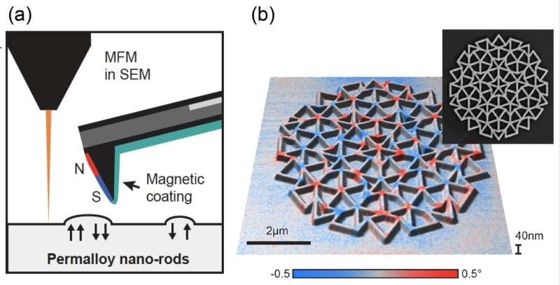
“It also extends the application of self-sensing AFM cantilevers into a broader range of surface characterization techniques, such as Magnetic Force Microscopy (MFM) or Kelvin Probe Force Microscopy (KPFM), where the cantilever’s surface must be coated with functional layers.”
As part of their recent work, Dr. Hosseini and her colleagues used their design to fabricate a prototype of a MEMS device. Initial tests showed that this device performed remarkably well, consistently detecting force and deflection in different environments.
“One of the standout achievements of this work is the fabrication of a MEMS device that combines high deflection sensitivity with mechanical robustness,” Dr. Hossaini said. “The combination of polymer core and doped polysilicon strain sensors allows the cantilever to detect very small forces.”
The newly designed cantilever was found to be highly robust and adaptable, thus it could have various real-world applications. For example, it could be used to detect mass changes in chemical and biological samples, thus aiding their characterization at a nanoscale.
In health care settings, the device could support high-precision diagnostics and the detailed monitoring of biological signals. Moreover, the cantilever could be used to monitor natural environments, detecting small but meaningful changes in pollution.
“Moving forward, we plan to continue optimizing the performance of these cantilevers by exploring new material combinations and refining their sensitivity and durability,” Dr. Hosseini added. “A key focus will be integrating them into more complex systems, such as microfluidic platforms, to expand their real-time diagnostic and monitoring capabilities.
“The prototypes of our multilayer cantilevers have already attracted interest from international companies, and I am actively fabricating these devices for use across various industries.”
Dr. Hosseini is making the cantilever introduced in her paper accessible to engineers and manufacturers worldwide. Within the next year, the researchers plan to launch a spin-off based on their patented design so that it can be used by semiconductor manufacturers and engineers developing medical technology.
© 2024 Science X Network
